Join high-purity PVDF water pipe the way a fitter joins ordinary plastic pipe and every fusion bead becomes a crevice for bacteria.
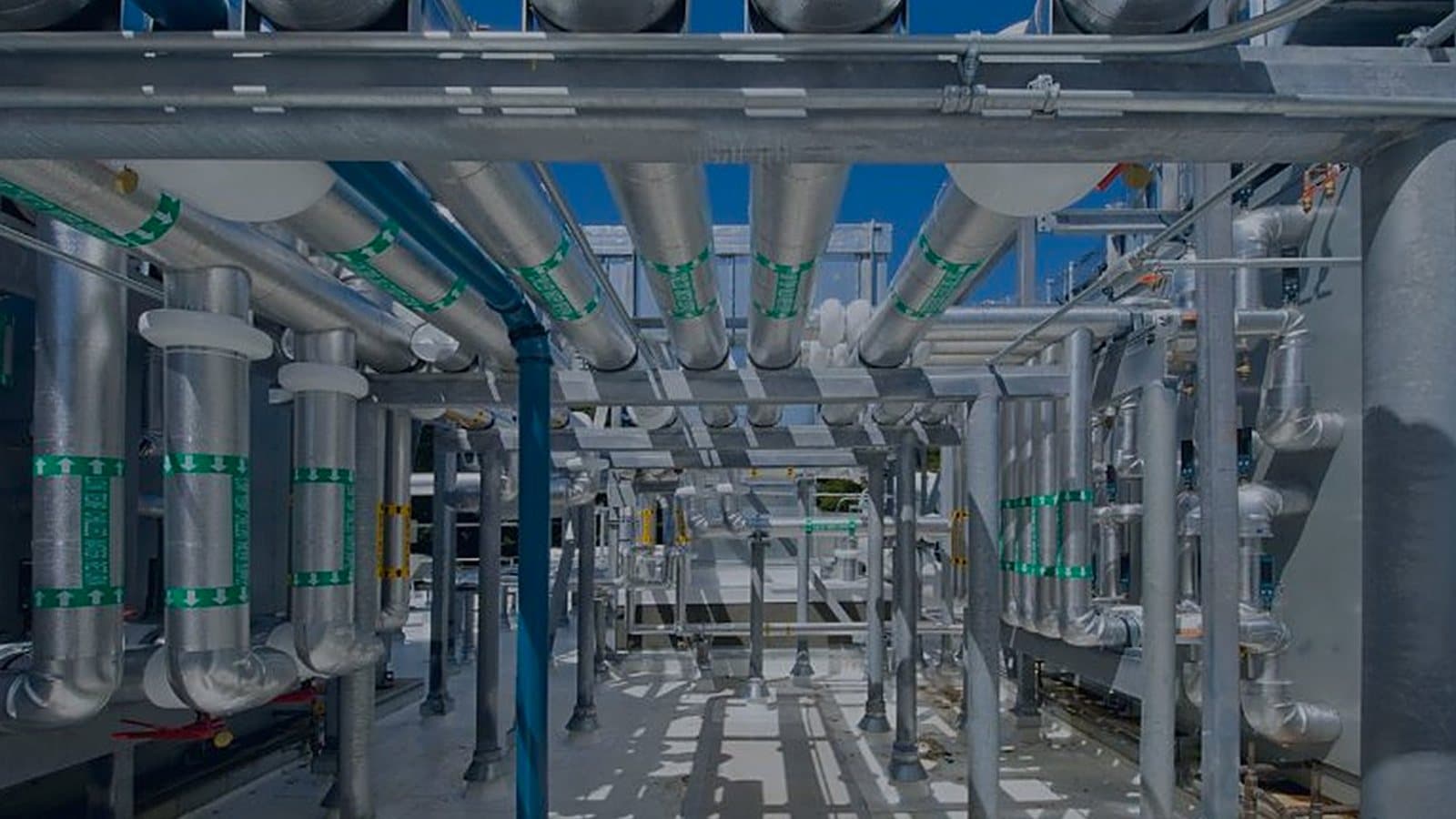
That is why ultra-pure water loops in a fab are joined with bead-and-crevice-free fusion. The joint is formed against an inflatable bladder inside the pipe, so the inner wall comes out smooth. The water in those loops is specified in parts per billion, and in a semiconductor plant the inside of the pipe wall is part of the wafer's environment. A crevice that would never matter on a cooling-water line sheds particles and grows biofilm straight into the process.
Gas lines follow the same logic in metal. They use electropolished 316L tube, orbital welds made under purge gas with a weld coupon kept as evidence, and assembly under clean conditions. Before a line is handed to the process tool it gets a helium leak test and outlet checks for particles, moisture and oxygen. An industrial line in carbon steel or 304 stainless would get a flush and a pressure test.
Pharma engineers will recognise a good part of this from WFI work: 316L, orbital welds, weld logs, passivation. The step up is at the outlet. Moisture and oxygen are measured at levels that need their own analysers, and a single sample point can hold up a handover.
We design clean utilities for pharma and UHP utilities for semiconductor.
Industries